Shrike FPGA Bitstream Generation Guide
Bitstream is a firmware that is used to programme the FPGA and map our design to it. Shrike uses a Renesas Forge FPGA SLGV SLG47910 1K Luts FPGA.The datasheet fr which can be found here .
For generating the bitstream for shrike we will use these steps.
Setup
Design & Synthesis
IO Mapping and Placement and Routing (PNR)
I am here assuming that you have installed all the tools required if not check tools_setup_guide HERE.
We will create a LED Blinking Project for this guide and we will start by launching the Go Configure Software Hub.
1. Setup
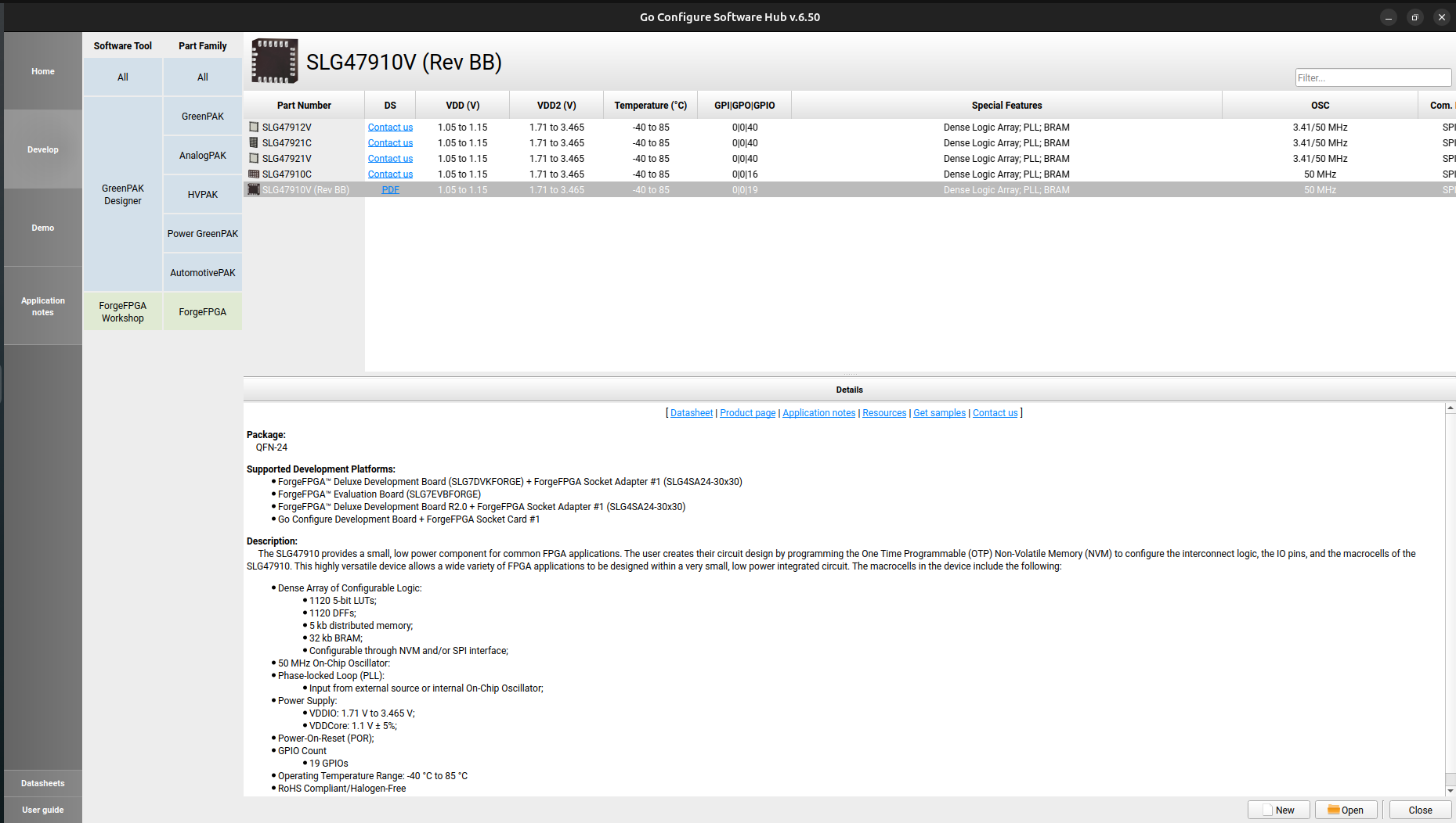
Launch the GO Configure Software Hub and move to the Forge FPGA tab under the Develop Tab.

Double click on the FPGA (SLG47910 (BB)) in our case. NOTE: You can also just open the led blink project available in the Projects section of github that can be done from the open option in the bottom right corner and then navigate to the ffpga file of that project.
Now select the project name and project location of your choice.
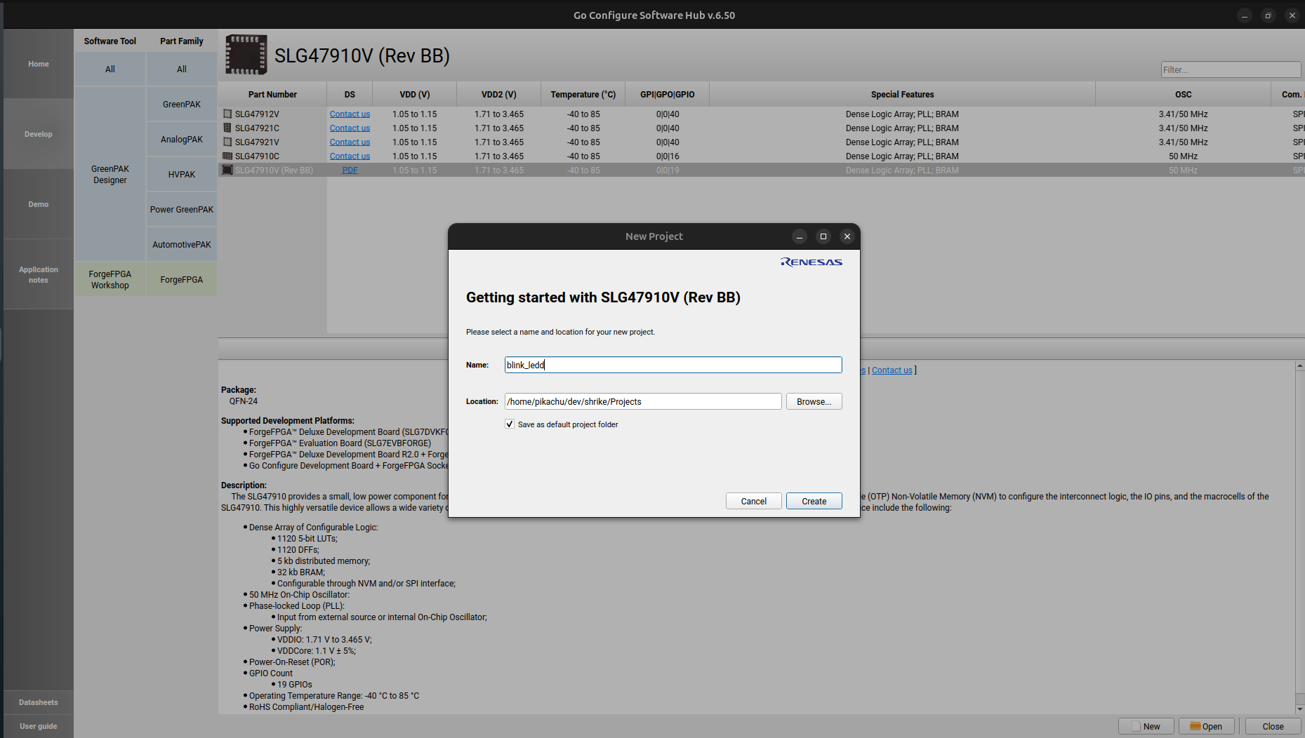
Now you will see the “Project setting” window select the first values in each box by clicking the arrow beside it. It should look like this.
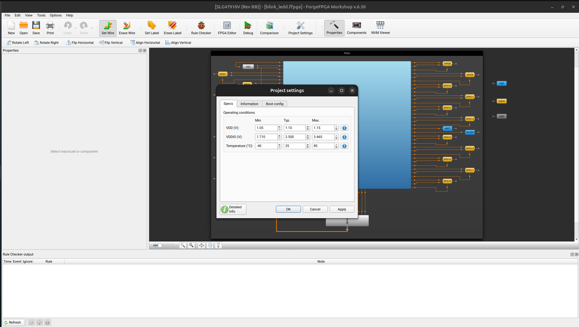
Double click on the light blue square (FPGA Core) in and you should see this window. Now you are done with setup lets design our blink led hardware.
Check out this short video guide.
2. Design
Now we will how we can design a led_blink hardware.
So as of now we are aware that we need a led that should be blinked so lets declare that in verilog.
module led_blink (output led,
                  output led_en);
endmodule
Now every output requires a output enable for forge FPGA thus we will define a led_en pin as well and we will keep it high ( value = 1) by default so that led signal ( IO) is always a output from the board.
We need to figure out a way to so how are we going to blink ( toggle ) this led , for convenience lets assume we want to blink it every second . So this tell’s us that we need some kind of clock to check the time and how much time has passed.
We have a clock on out FPGA it is a pulsating signal that creates a 50Mhz square wave, we have to use this to calculate one second to do so we can simply add a counter that counts till 50_000_000 cycles as that how much we will require to reach one second at a 50 Mhz frequency.
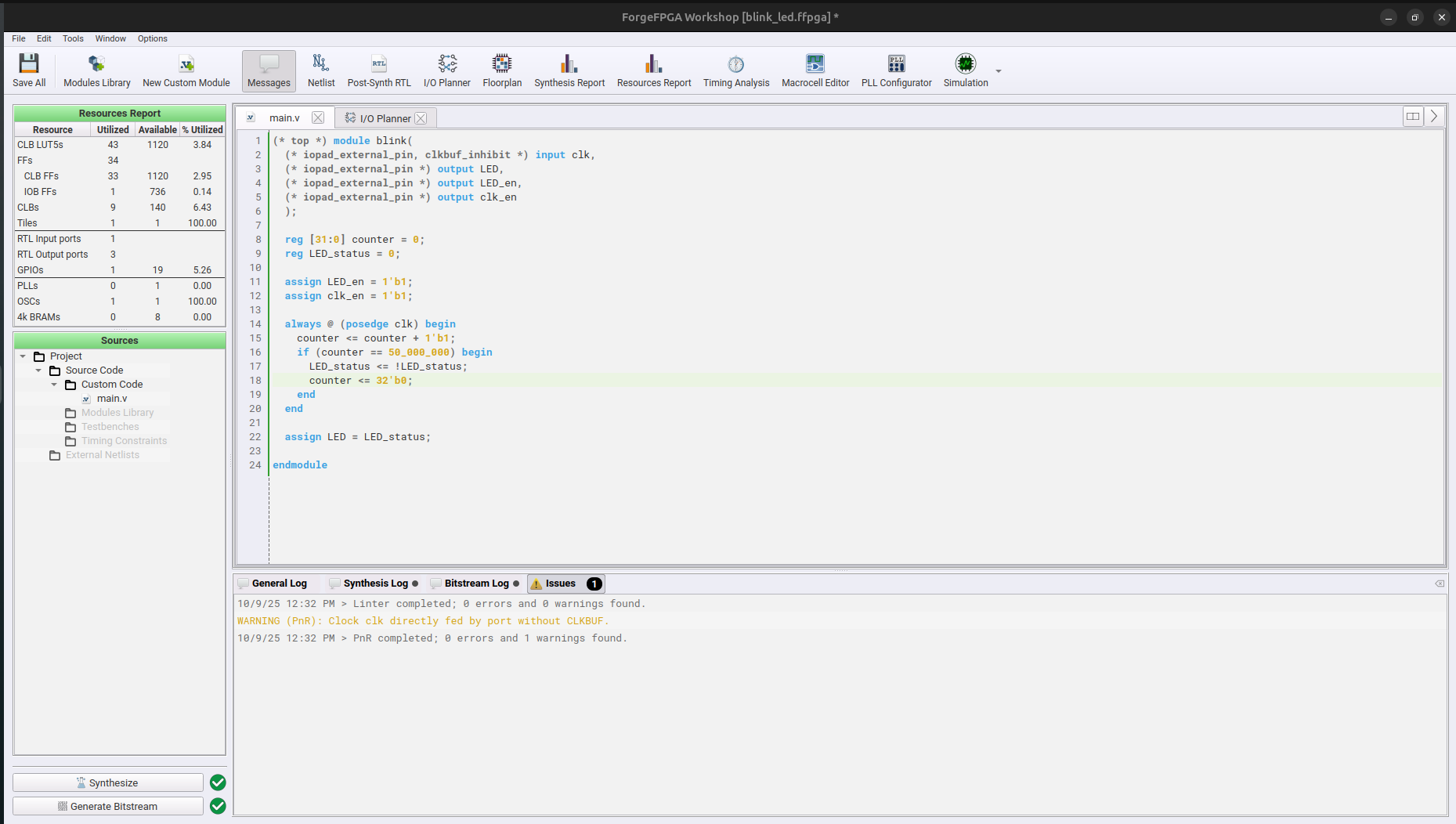
Thus now we will create a hardware that blinks a led whenever its counter reaches 50_000_000 and the verilog for this will look like this
(* top *) module blink(
  (* iopad_external_pin, clkbuf_inhibit *) input clk,
  (* iopad_external_pin *) output LED,
  (* iopad_external_pin *) output LED_en,
  (* iopad_external_pin *) output clk_en
  );

  reg [31:0] counter;
  reg LED_status;

  assign LED_en = 1'b1;
  assign clk_en = 1'b1;

  always @ (posedge clk) begin
    counter <= counter + 1'b1;
    if (counter == 50_000_000) begin
      LED_status <= !LED_status;
      counter <= 32'b0;
    end
  end

  assign LED = LED_status;

endmodule
There are a lot other ways to blink an led as well and you can always use those however before writing verilog for shrike please checkout Style Guide for reference .
However here we are assuming that you are using the code mentioned above . Get this code in the main.v in the software.
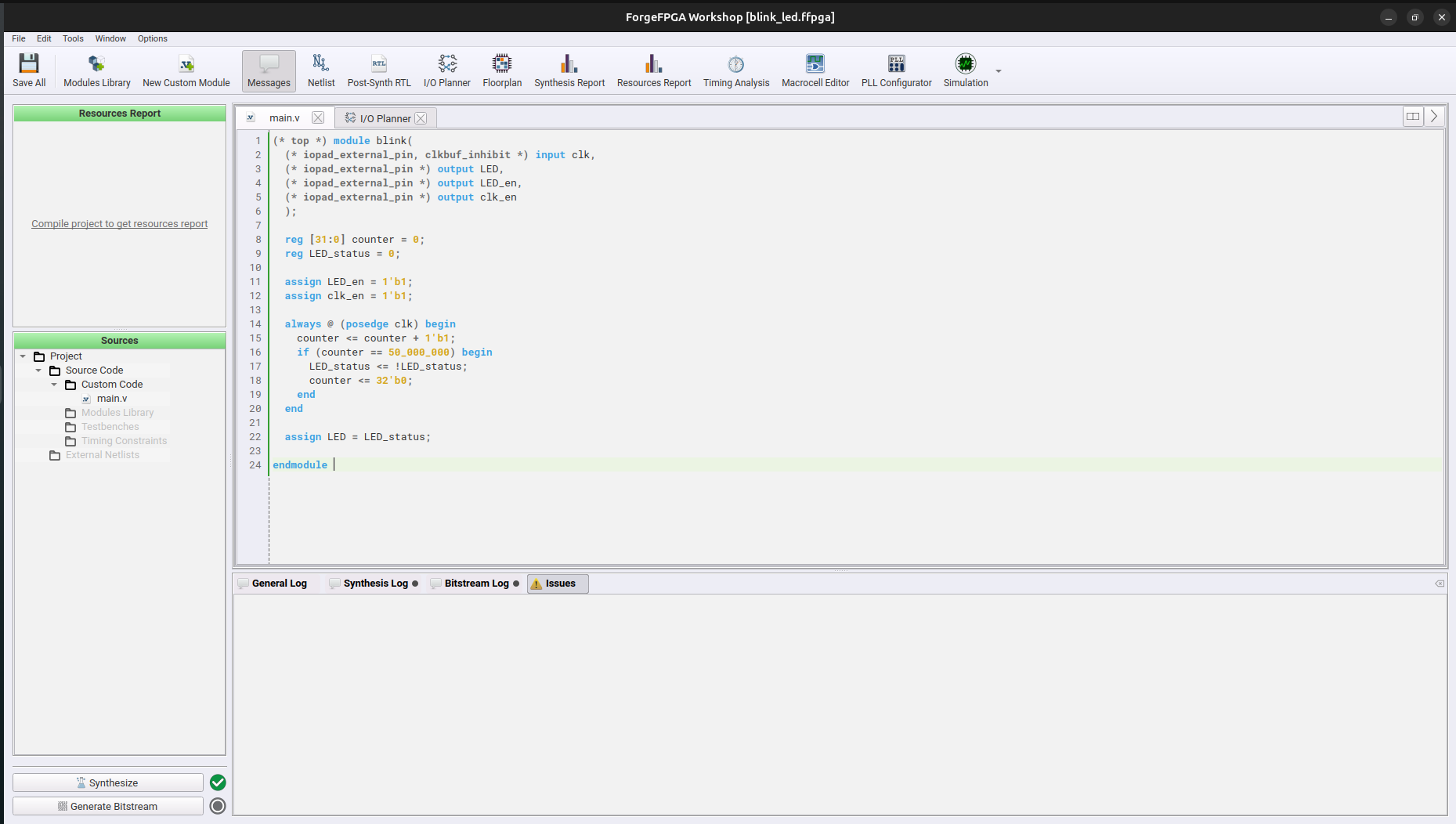
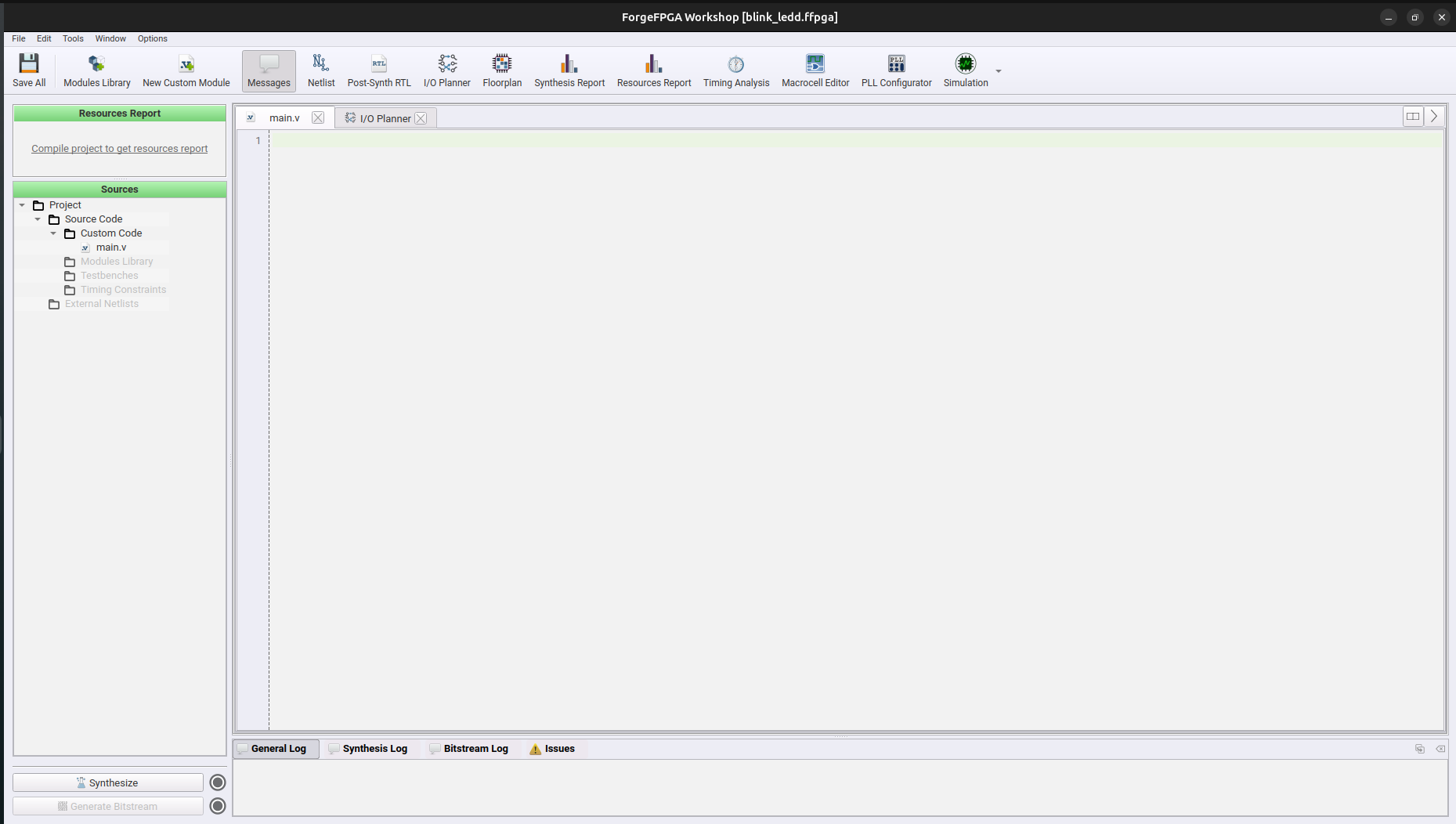
Now the next step will be to synthesize the verilog for doing so click the button in the bottom left corner. It should take a minute and then you will a green tick beside it that should tell you that synthesis has happens without any error.
Now we will move to IO planning and bitstream generation.
3. IO Planning and PNR
Now that we have synthesized the verilog lets connect the signal to the Input outputs pins. Follow the command below to map the required pins.
Open the IO planner from the top bar in the software.
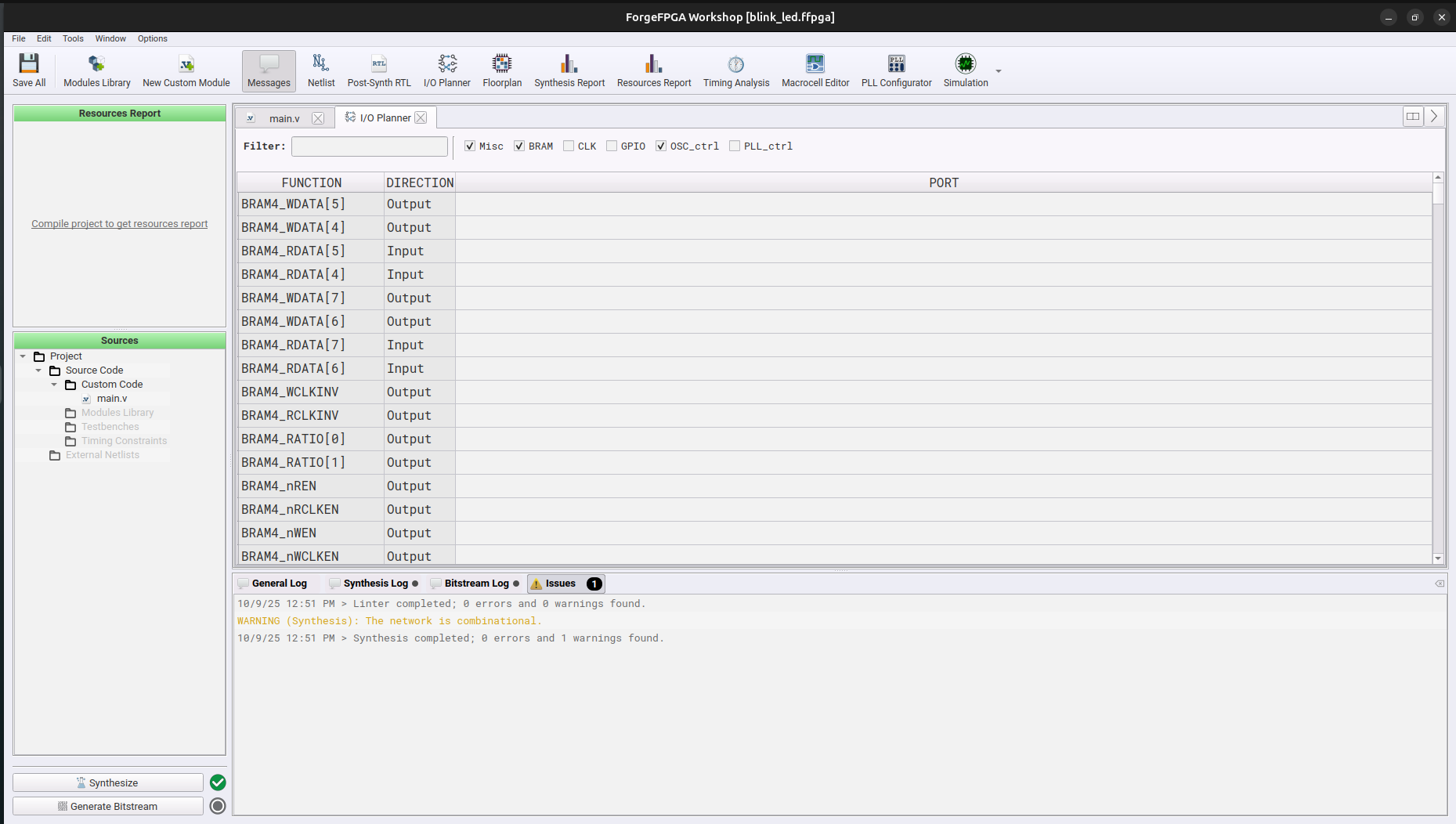
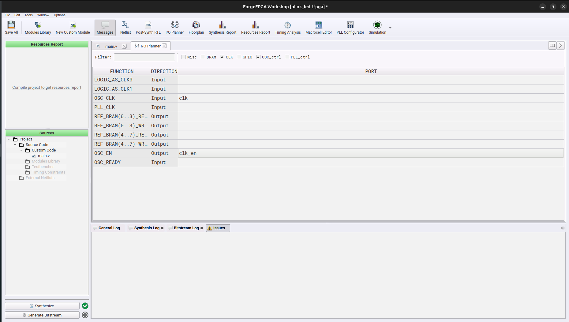
Now we will first map the clock pins , filter the selection by using CLK and OSC_ctrl tab.
We have two clock related signal “clk” and “clk_en” map them to “OSC_CLK” and “OSC_EN” respectively.
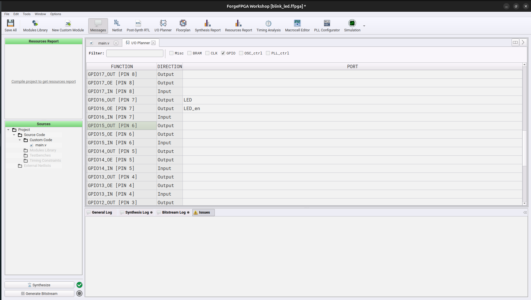
Lets map the led out signals , filter the selection , select only the GPIO , un-tick all the other onces.
We have two signal related to led “LED” and “LED_en” as output, on shrike led is connected to pin number 16 we will connected these signals to “GPIO16_OUT” and “GPIO16_OE” respectively.
IO planning has been done save the setting and press Generate Bitstream button in the left bottom . It will take some time to generate bitstream and you will see a green tick after its done.
Congratulation’s you have generated your first hardware.
[!NOTE] The bitstream file that you need to copy will be named as “FPGA_bitstream_MCU.bin” found in ffpga -> build -> bitstream folder in your project directory.
If you copy any other file present in the bitstream folder the fpga wont be programmed. You are free to change the name of this file however you please.
Now that you have generated your first bitstream let’s upload these on the FPGA, that will be pretty simple follow the step 3-4 in this guide or complete guide if you checking it for first time getting_started .
Check out the Verilog Style Guide next.